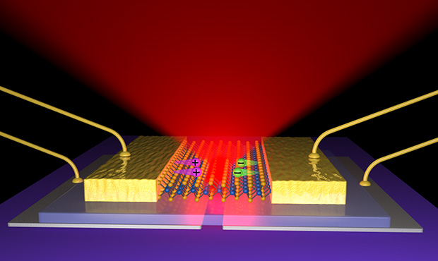
Think your LEDs are small now? New research coming in from the University of Washington is showing the development of LEDs that are three atoms thick. How thin is that? About 10,000 times thinner than a human hair. That’s pretty thin!
The LED itself is made from slightly different materials than we are used to seeing in our usual selection of LEDs. Tungsten diselenide is at the heart of this device, being what they call a “molecular semiconductor”. This material is so thin, it falls into the category of “two-dimensional materials”, which we are having a hard time with considering it’s three atoms thick, but we aren’t the physics pros. Being so thin though, it makes the structure flexible, transparent, and quite durable, leading to many interesting possible uses. We aren’t expecting these to be as efficient as current generation InGaN and GaN based LEDs, but it’s early days yet.
So what uses would something like this have in the world of aquaria? Not a lot really, at least for the immediate future. The big promise for this technology is light based computing. Replacing the nanoscale wires in computer chips with light can dramatically increase the speed and efficiency of the device, leading to far more complex and powerful products that use a lot less energy. Could we see light based chips in our system controllers in the future? It’s almost a certainty, but “when” is the key question.
As for the lighting side of our little part of the world, this technology might not apply directly, but the evolution of this technology may lead to some interesting designs. The flexible nature of this device could lead to fixtures that are easy to bend and shape to put light where you need it without having to resort to (relatively) inefficient secondary optics. The transparent nature of the device could also mean that lighting products could be completely see through when off (maybe even when on too), or even built into the glass surfaces of the aquarium to provide light. It might be a bit of a stretch to think of applying the technology in this way, but breakthrough products are created by those who think a little outside the box when it comes to applying these concepts to designs, so almost anything really is possible.
What is interesting about this announcement is more the molecular semiconductors than the three atom thick LED itself. With diodes (and of course LEDs), the semiconductor material is doped with various dissimilar materials to create the p-type and/or n-type junctions at the heart of the device. These molecular semiconductors, tungsten diselenide in particular, acts in a very similar way to these doped semiconductors by just bringing the super thin material into close proximity with a metal electrode, and changing the polarity to change it from n-type to p-type. This alone allows you to create the perfect diode, regardless of the application, on demand.
In addition to that, and something that’s more applicable to LEDs, the material can be tweaked to change it’s band gap properties. The band gap defines the wavelength of light that is emitted from the LED, and is usually limited to certain wavelength ranges based on the materials used. Tungsten diselenide could be engineered to produce almost any wavelength of light, which could open up a huge range of possibilities for lighting, possibly including the LED holy grail of a true white LED.
Fortunately, it seems as though this technology has a bright manufacturable future ahead of it, unlike a lot of other lab based breakthroughs. Because this is using known semiconductor materials, LEDs and diodes based on this technology can be produced using standard semiconductor manufacturing techniques and machinery. We aren’t going to be seeing 3 atom thick LEDs next week, but it’s certainly possible to see this technology trickle into our everyday lives in the coming years rather than decades.
[phys.org]


